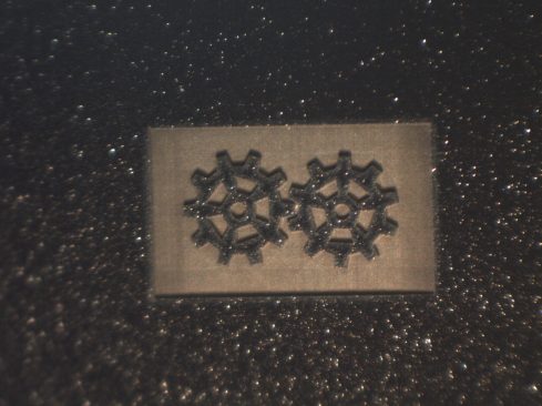
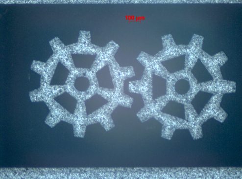
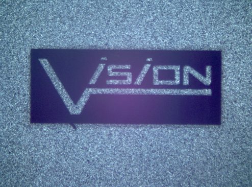
Today, laser marking on silicon is the current state of the art and a well established and widely used technology.
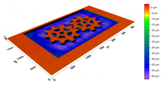
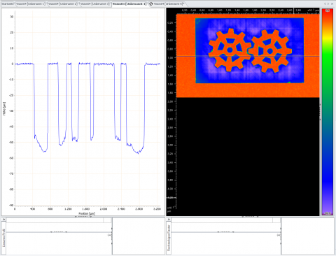
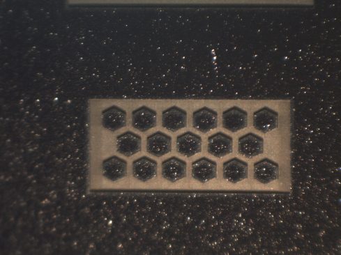
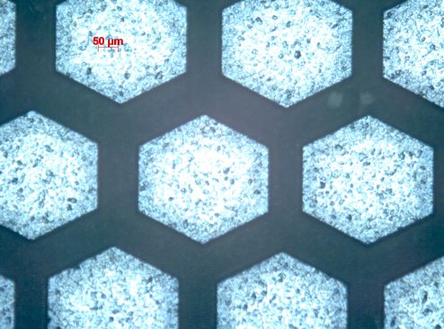
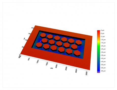
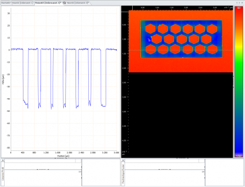
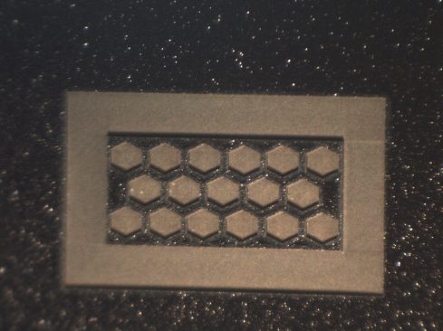
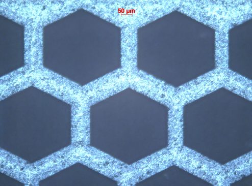
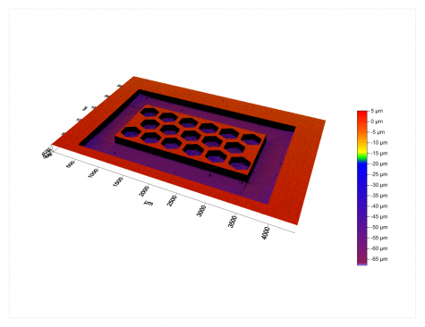
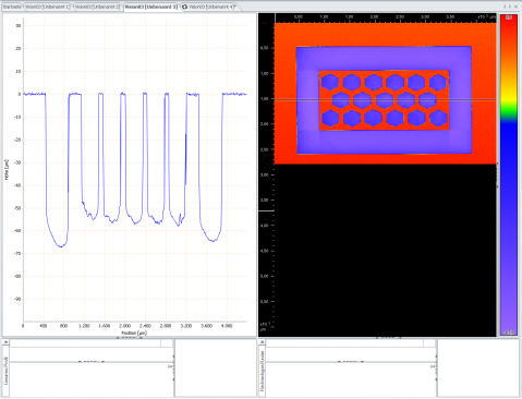
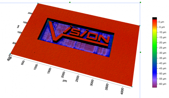
3D micro material processing with an accuracy of 0.01 μm, however, is one of the latest developments of Vision Lasertechnik GmbH.
A combination of 3D laser scanners in connection with mechanical axes ensures an accuracy of 1 μm.
The fully automatic 3D laser system for structuring of silicon wafers is the first influential system that forms the foundation for new challenges and many additional options and possibilities.
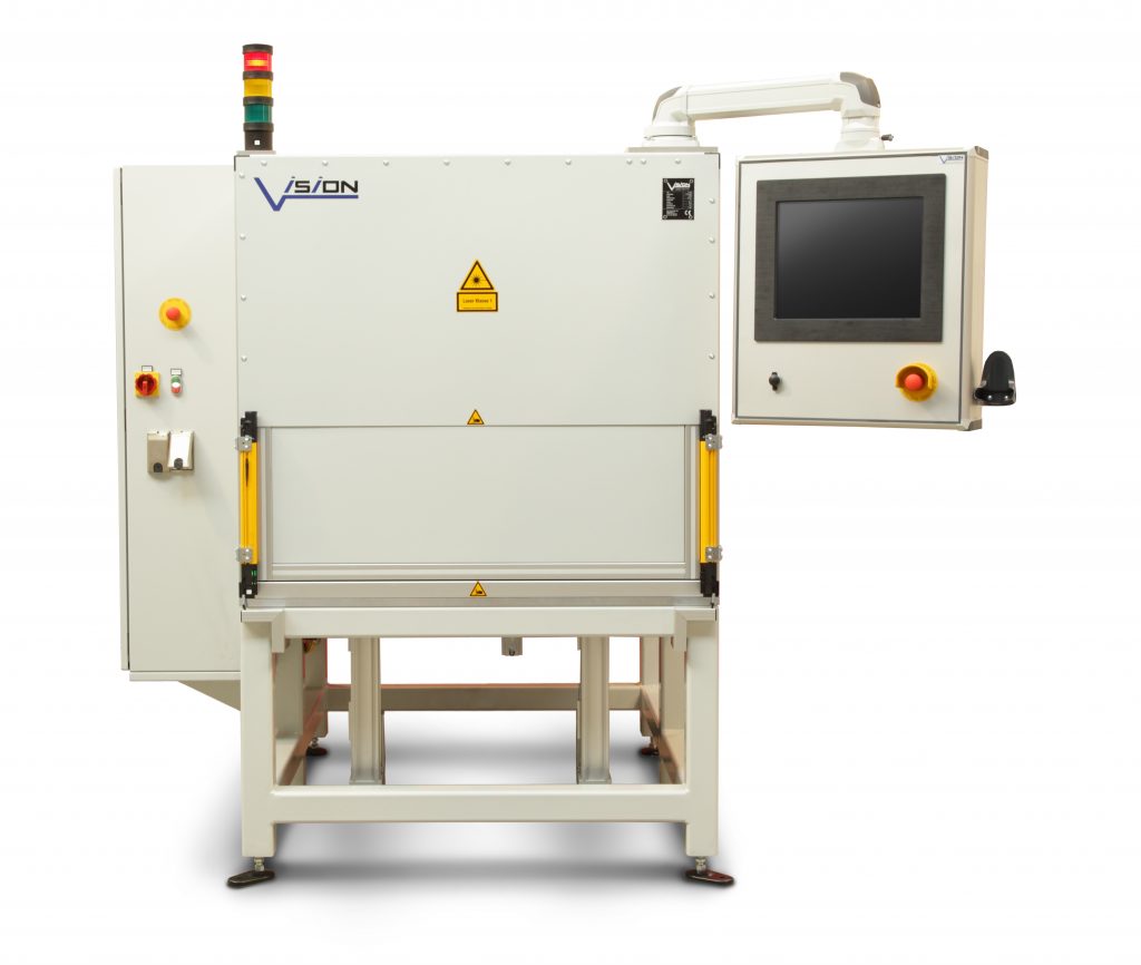



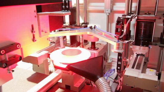


The presented machine is intended for fully automatic wafer processing from carrier systems.
After positioning the populated carriers, the machine unloads and loads the wafers automatically and the process is carried out fully automatically.
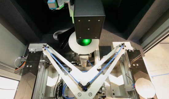
Wafer handling is performed with the use of highly precise vacuum suction cups so that even sensitive surfaces are ensured not to be damaged or scratched.
The system is capable of adjusting to various wafer thicknesses extremely quickly by means of an optical Z-axis.
Orientation of the wafers, as well as position scanning and correction is implemented by means of a high-resolution CCD camera system.
A special exhaust system protects the wafers from contamination by silicon dust; at the moment, the system can be extended to wafer sizes up to 12“.
Contact us to discuss new challenges. We will try to find a solution for your tasks.
If required, we will push the limits – that is our passion.
